


电子器件压缩模型在预测战术导弹中暂态热传递方面的应用
日期:2012-06-19
Application of Electronics Compact Models to the Prediction of Transient Heat Transfer in Tactical Missiles |
|||||||||||||||||||||||||||||||||||||||||||||||||||||||||||||||||||||||||||||||||||||||||||||||||||||||||||||||||||||||||||||||||||||||||||||||||||||||||||||||||||||||||||||||||||||||||||||||||||||||||||||||||||||||||||||||||||||||||||||||||||||||||||
|
Karen L. Alibrandi, Marcelle S. Ibrahim and Leo R. Paradis Thermal design of electronics systems used in tactical missiles must make use of thermal capacitance to limit critical temperatures to acceptable levels. Since the classical qJ-C electronics package thermal characterization does not address package capacitance, detailed models of the packages and boards must be constructed and solved in order to estimate correctly the capacitance available for thermal control. The new approach to thermal modeling, in which the vendor supplies a simplified and calibrated thermal model, now universally known as compact modeling, offers some promise of streamlining this process. However, for the most part, the models being developed and discussed in the literature are resistor networks used to predict steady state operating temperatures; little attention has been paid to solving the time-dependent heat transfer problem. Raytheon Electronic Systems Laboratories has studied the application of the Compact Model approach to an idealized missile electronics transient problem. Flomerics, Inc. provided a Detailed Model of a 208-pin Plastic Quad Flat Pack and a calibrated Compact Model of the same device for use in the study. After installing the models on Raytheon computers and becoming familiar with them, package capacitance was added to the compact resistor network at specific locations, and both models were exercised for transient operation. The results indicate that the Compact Model approach lends itself very well to solution of the transient heat transfer problem. It is recommended that model providers include geometry and capacitance information commensurate with the validated model, thereby allowing it to be used in either the steady state or transient mode. DiscussionProblem Description The problem of designing electronics for most tactical missile applications poses many challenges to the thermal designer/analyst:
Solution of the thermal problem requires that detailed models of packages and boards be constructed and exercised for derived boundary conditions, a time consuming process. Frequently, component manufacturer-supplied qJ-C data is not suitable for the task, since it does not address package capacitance, nor does it develop the intra-package resistance terms that are required to accurately locate the package capacitance in the model. Numerous investigators have addressed these shortcomings and have identified approaches that may lead to their amelioration in the future [1, 2, 3]. The Compact Model (CM) has since evolved, and appears to be gaining acceptance, with spirited discussion regarding the particular CM approach to be utilized [4, 5]. For the most part, model development and validation activities have concentrated on steady state solutions to the heat transfer problem, as this represents the principal operational concern of most users. With the exception of the work of Christiaens et al [6, 7], there appears to be little in the open literature concerning transient solutions utilizing the compact approach. Also, there appears to be little or no independent user evaluations of the various CM's being developed, steady state or transient. This paper reports on a study performed on the applicability of the CM method to a problem that arises frequently at Raytheon Electronic Systems (RES), that of transient temperature control in a high temperature environment, as exemplified by air interceptor missiles.
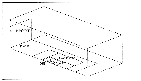
The nature of the study mandated that a Detailed Model (DM) and CM of the same package be available for analyses. The Flomerics Company has been very active in the development of Compact Models [8], and the FLOTHERM computer program, V1.4, [9] is in wide use at RES. Upon our request, technical representatives in Flomerics' Marlboro, MA office provided the authors with models of a 208 pin, Plastic Quad Flat Pack (PQFP), as described below [10,11]. This generosity on Flomerics' part was greatly appreciated, as it provided all the requisite information for the study to proceed. The detailed model of the 208 PQFP received from Flomerics was part of a system which consisted of a printed wiring board supported inside an enclosure, as shown in Figure 1. This model is very similar to that described in reference [12].
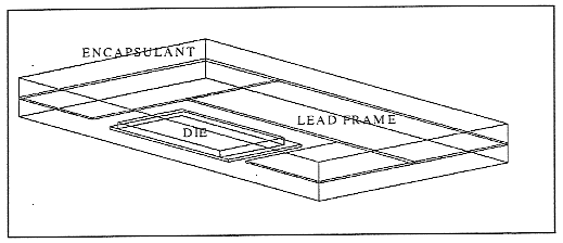
Figure 1 - Flomerics' system level model of a board mounted, 208 PQFP The model is comprised of a number of cuboidal volumes which represent: the package encapsulant (case), the die and die attach, lead frames and leads, the board, and ambient air. Each volume was assigned a thermal conductivity in the model, and these were retained without modification for this study. Cuboid density and specific heat were added at Raytheon, after consultation with Flomerics. All thermal properties used in the study are summarized in Table1. The model was designed originally to include the study of convective flows within the system via FLOTHERM's CFD routines. This capability was not required for the current study, which planned to impose boundary conditions taken from Lasance. Therefore, a package only Detailed Model was developed by deleting the system level components and adding external plates over all the exposed package surfaces to act as convective surfaces to the ambient. In addition, heat flow from the leads was not included in the detailed model for simplicity sake in forming the package convective surfaces. This approach should lead to an insignificant increase in predicted package temperatures, but would not impact the conclusions of the study, since the same assumption was used for both the DM and the CM. The package Detailed Model resulting from these modifications contained a total of 6 volumes, and utilized a plane of symmetry along the Y axis to reduce computational time, as shown in Figure 2. The power dissipation was applied on the surface of the die using a planar source input of 0.5W for the half model.
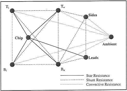
The Flomerics-provided and RES-modified Detailed Models were exercised for both free and forced convection and transient and steady state scenarios in order to check the models and gain experience in their use. Following that, the Lasance boundary conditions described below were imposed on both models and exercised in both a steady state and transient mode, with results as reported below. A calibrated Compact Model of the 208 PQFP was also provided by Flomerics [11]. This resistor based model has been validated for steady state operation against the set of 38 boundary conditions defined by Lasance [4]. The CM was modeled in PC3D [13], a finite difference thermal analyzer capable of both geometric and/or network modeling. Although FLOTHERM 1.4 was considered, its use for RC circuit analysis in the transient mode was felt beyond the scope of the current activity, which possibly would have required generating cuboids for some of the shunt resistors, a formidable task. A decision was made to revisit this approach when FLOTHERM version 2.0 is available, as it has been reported to be more adaptable to the use of RC networks. The CM consisted of seven nodes representing the junction, the sides, the leads, and the package top and bottom, each split into two nodes: the inner and the outer. The surface area associated with each node was also provided by Flomerics. In the CM, these areas are essential for applying the boundary conditions to the model. The nodes were connected by a total of 16 star and shunt resistors, each of which is defined in Table 2. In addition, the convecting nodes were coupled to a constant temperature node representing the ambient. The resistor network for the resulting CM is shown pictorially in Figure 3.
As previously stated, the goal of the analysis was to study the applicability of the CM to solving transient thermal problems. The CM provided no information as to how package capacitance terms could be distributed among the principal or star resistors. It was estimated that trying to distribute the package capacitances among the star and shunt resistors, per some schedule, would result in a large number of perturbations that possibly would never be solved correctly. Therefore, the decision was made to distribute the total package capacitance among the top, bottom and side surfaces in proportion to their surface areas, with a very small capacitance assigned to the chip and leads. The entire package volume, taken from the DM, is 2.352 cm3, and the overwhelmingly predominant material is encapsulant. Thus, the entire package capacitance was assigned a value of 3.776 J/K, using the properties in Table 1. Since there was no indication of how much volume should be assigned to the sides relative to the top and bottom, an 80% to 20%, top and bottom to sides, ratio was determined somewhat arbitrarily. Thus, the top and bottom would have a total capacitance of 3.20 J/K, and the sides' capacitance would be 0.76 J/K. By further area weighting, the top and bottom inner and outer capacitances were determined to be 0.29, 1.52, 0.19 and 1.0 J/K, respectively. If transient results mandated, the proportions could be changed appropriately during later analyses.
The boundary conditions to be used in the analysis were selected from the Lasance grouping of 38 described in [4], see Table 3. A subset of four of the boundary conditions were selected for the purposes of the study, per the rationale that follows.
These boundary conditions were applied to the detailed and compact models in both the transient and steady state mode, as described Table 4.
The DM and CM were first run in steady state solutions for the boundary conditions to establish the degree of comparison with each other. Table 5 presents the results of the comparison, including using the chip temperature predictions of each model to form the input to a percentage difference evaluation. The chip temperature differences between the models were not large, and the agreement between the models was determined to be adequate for the purposes of the study. Therefore, no efforts were expended to attempt to minimize or further evaluate the differences.
* % Difference = 100 x (TCM - TDM)/( TDM - TAMB) The next series of analyses investigated the transient response for each model. The application of the CM capacitances described above was first applied at the location of each node representing the bottom, top, etc., separated by the star resistors. Evaluation of those results indicated that moderate differences between the DM and CM were developing early in the analysis, which ultimately resolved to the steady state differences shown above. The first approach to resolve the differences consisted of halving the star resistors, establishing a node at the intermediate location, and applying one half of each capacitance term to the intermediate node. The remainder of the capacitance, i.e., one half of the former value, was retained at the each original node. This new resistor network is depicted in Figure 4, with the resistors summarized in Table 6. The results of all of the transient analyses are presented in Figures 5 through 8.
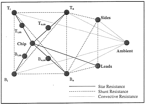 Figure 4 - 208 PQFP Compact Model Star/Shunt Resistor Network with Distributed Capacitance Terms
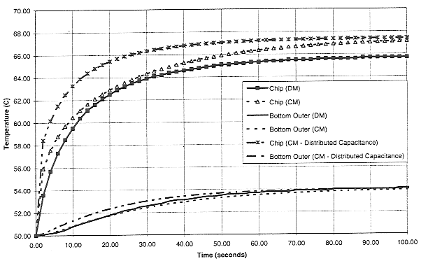
Figure 5 shows chip junction and package bottom, outer time/temperature histories for boundary condition No. 37 for the first 100 seconds of operation. A chip junction temperature difference between the models of 3 - 4°C developed early in the case when using the concentrated capacitance approach, which gradually diminished as time progressed, finally attaining the expected steady state temperature differences. In contrast, the distributed capacitance CM matched the DM response much more closely, until the steady state was nearly established, at which time there was little difference between the two CM's. The package nodes behaved in a similar manner, with the distributed capacitance results comparing nicely with the DM results throughout the analysis.
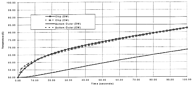
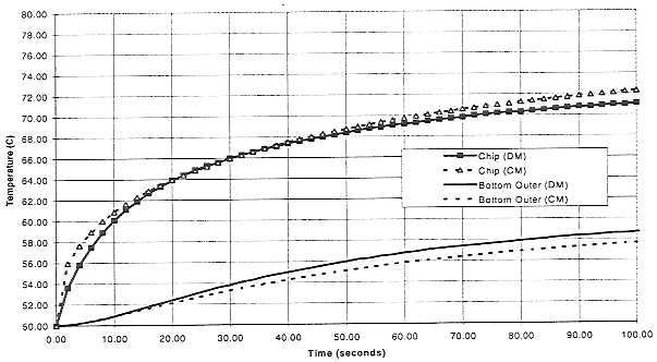
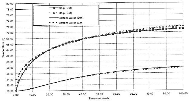
Figure 5 - Transient temperature response comparison between two Figures 6, 7 and 8 demonstrate similar results for the three remaining cases. In each, a fairly coarse capacitance reallocation provided a very good agreement between the CM and the DM, and these probably could be improved upon, if that were necessary. For the case at hand, however, the applicability of the CM approach had been demonstrated, and there was no need to proceed further at this time.
Figure 6 - Transient temperature response comparison between Distributed Capacitance
Figure 7 - Transient temperature response comparison between Distributed Capacitance
Figure 8 - Transient temperature response comparison between Distributed Capacitance In conclusion, the thermal analysis presented demonstrates that the CM approach is amenable to the solution of typical applied transient problems with a minimum of modifications to incorporate system capacitances. This conclusion is in agreement with reference 7, which took a more mathematical intensive approach to the problem. It was reassuring that the application of some fairly logical modeling assumptions regarding the location of capacitance terms in a RC thermal network achieved such favorable results so quickly. It is recommended that CM developers include sufficient data such as package surface area, package capacitance terms and where they should be located in the nodal network to support users who are addressing transient problems. This information would seem to flow readily from the Detailed Model, and thus would be easily obtained by the CM developer. Acknowledgement
The authors would like to acknowledge the help of Andre Ali for providing the models used in this work; and Clemens Lasance and Eric Beyne for providing us with up-to-date information on the subject, and to Smita Munroe for her assistance in developing and processing the data presented herein.
|
|||||||||||||||||||||||||||||||||||||||||||||||||||||||||||||||||||||||||||||||||||||||||||||||||||||||||||||||||||||||||||||||||||||||||||||||||||||||||||||||||||||||||||||||||||||||||||||||||||||||||||||||||||||||||||||||||||||||||||||||||||||||||||

 沪公网安备 31010602003953号