|
Networking companies continually face tremendous pressure to bring to market the latest products and technologies. As a result, EMC design issues are moving quickly past levels supported by traditional design processes. Two short years ago, EMC issues were secondary considerations. Today, market leaders spend tens of thousands of dollars on weeks in the anechoic chamber. They also risk hundreds of thousands of dollars in opportunity costs solving complex EMC issues for optical transceivers using traditional means. The growing EMC problem coupled with a shrinking design cycle has placed a premium on advanced, low-cost techniques for EMC design.
EMC issues for optical transceivers must be considered at two levels. For the transceiver itself, high frequency radiation can leak from holes, gaps and seams that are inherent features of transceivers. This in itself is not a problem in that sub-systems are not subject to emissions standards. However, problems emerge when electromagnetically "hot" transceivers are placed into systems that are bound by emissions limits. Radiating transceivers couple to air vents, cavities, seams and holes that are inherent features of systems. They also are often are mounted externally on a system. This breaks the integrity of the enclosure shield and causes them to effectively behave like antennas, amplifying energy generated inside systems and then transmitting to the outside world. Both effects are common. Accurate analysis of the transceivers themselves and their effect on a system could mean the difference between passing or failing FCC (US) and CE (EU) emissions compliance tests.
This article addresses the issue of radiation from small form factor pluggable Optical transceivers when modeled as a single device mounted on a PCB and also when modeled as multiple devices enclosed within a metal enclosure.
The type of transceiver considered here is commonly used by many companies to provide high-speed optical connections between systems, typically in the range of 1 to 2.5 Gbps. To enable different transceivers to be used in different systems a Cooperation Agreement was drawn up which defines the aspects of the transceiver design:
-
Transceiver package dimensions
-
Mating of transceiver PCB to electrical connector
-
Host PCB layout
-
Insertion, extraction and retention forces for transceivers
-
Labeling of transceivers
-
Bezel design for systems using transceivers
-
Electrical connector mechanical specifications
-
Transceiver cage assembly dimensions
15 companies including Agilent Technologies, Hitachi Cable, IBM Corporation and Tyco Electronics signed this cooperation agreement.
All the transceiver models presented in this article are based on the above agreement.
FLO/EMC Model Details
In a real system employing optical transceivers the geometry is highly complex involving small details, multiple layer PCB's and vast numbers of components on the PCB's along with complex track paths. To model all of this detail would take a tremendous amount of time and lead to large models with very long run times, so the transceivers and the PCB's on which they were mounted were simplified to reduce this detail. All the PCB's in the system were modeled as solid copper sheets and the only detail on the PCB's that were modeled was the chips located within the transceiver that drives the optics. The justification for this simplification is detailed in [1] which discusses the modeling of boards connected to a backplane.
Two models of the transceiver were developed the first being a single device mounted on a PCB, and the second being a group of 5 transceivers mounted on a PCB within a metal enclosure. In both models the sources were the drive chips located on the PCB within the transceiver, and these were excited with initial field sources. Figure 1 shows the models used in the FLO/EMC simulation.
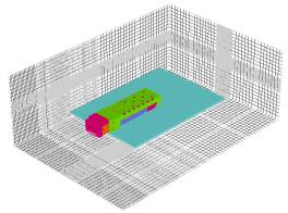 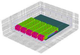
Figure1: FLO/EMC Models Used, Single Transceiver, Grouped Transceivers
Single Transceiver Results
The outputs for the single transceiver were monitored at the following frequencies, which were known to be problem frequencies with small form factor transceivers:
3.2 GHz
7.4 GHz
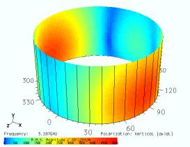
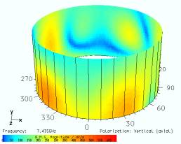
Figures 2 and 3 shows cylindrical profiles of the emissions produced by the single transceiver at the two frequencies listed above. The cylindrical profiles shown are at a distance of 3 meters from the transceiver and simulate an antenna scan height of 3 meters, which is in accordance with the test methods currently specified in EMC standards around the world where the device under test (DUT) is rotated in relation to the antenna and the antenna is scanned in height to determine the maximum emissions from the DUT. This type of output enables the user to determine the direction of the maximum emissions, which can be ultimately used to determine where design modifications need to be made to the DUT and also help the test engineer to find the maximum emissions during pre-compliance testing. From the cylindrical profiles it can be seen at these two frequencies the worst position for the emissions is from the side at 3.2 GHz and at 7.4 GHz the worst location was at 30o from the front of the transceiver. These locations for the maximum emissions correspond well with measured data.
|
|
Figure 2: Cylindrical Profile, 3.2 GHz
|
Figure 3: Cylindrical Profile, 7.4 GHz
|
Figures 4 and 5 show the electric field pattern produced by the transceiver at the same frequencies, at both frequencies the field was monitored with a horizontal plane through the center of the transmit / receive ports.
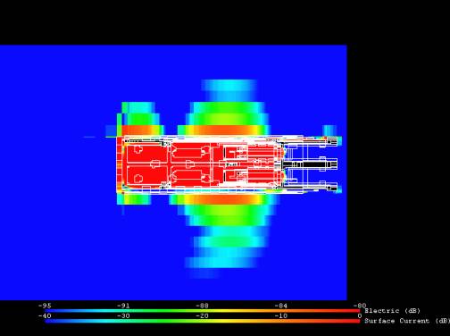
Figure 4: Electric Field at 3.2 GHz
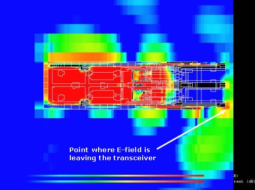 Figure 5: Electric Field at 7.4 GHz
The field profiles enable a user of FLO/EMC to understand how the fields are escaping from a device and to focus any design modifications that need to be made in the correct area. For example at 7.4 GHz the field profile shows how the electric field is escaping from the front of the transceiver, but the point at which the field is exciting is not directly from front but at the corner of the device. Further investigation of these output files would enable a designer to fully identify the path the field was taking and enable corresponding design changes to be implemented.
Grouped Transceiver Results
The grouped transceiver model was used to try and understand what happens when firstly the transceivers are grouped together and secondly how the emissions profile changes when they are encased within a metal enclosure with the correct bezel as defined in the cooperation agreement.
Figure 6 shows the field profile monitored from the front of the enclosure (where the bezel is located). These results showed that the prominent resonance was still at 7.4 GHz that was the one of the resonances investigated with the single transceiver. Due to this all the additional analysis in this article will be centered on this frequency. Discussions with a user of these types of transceivers confirmed that the resonance's that were being seen in the model corresponded with those seen in the measurement chamber.
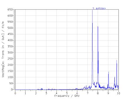
Figure 6: Electric Field Profile Monitored From the Front of the Enclosure
Figure 7 shows the cylindrical profile of the grouped transceivers at the frequency of 7.4 GHz. This result shows that the addition of the metal enclosure around the transceivers with the bezel on the front causes the radiation profile to be directed more from the front of the transceiver, with the maximum emissions now being at 0o, which corresponds to the location of the bezel. The radiation profile was also predominantly vertically polarized with virtually no emissions seen in the horizontal polarization.
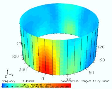
Figure 7: Cylindrical Profile of Grouped Transceivers at 7.4 GHz
As the system modeled here comprised of a group of the transceivers initially modeled, the results obtained previously could be applied here to identify the path taken by the electric field and implement corresponding corrective measures to the enclosure and the transceivers.
Conclusions
This article has presented the capability of FLO/EMC in solving problems with complex geometry, and also how FLO/EMC can be used to investigate problems at both a component and system level.
An in-depth understanding of the electromagnetic interactions inside optical transceivers and between transceivers and their environment is critical for effective design of high performance optical networking products. Virtual-prototyping early in the design process is a key aspect of effective design. The design information generated for the optical transceiver in this example took only a matter of hours. Generating this amount of data would take days in the lab and the information gathered would much less complete. Similar benefits can be realized for EMC design of complete systems.
References
[1] K. Li, M. Tassoudji, S. Poh, M. Tsuk, R. Shin and J. Kong, "FD-TD Analysis of Electromagnetic Radiation from Modules-on-Backplane Configurations", IEEE Trans. Electromag. Comp., Vol. 37, No. 3, Aug 1995, pp. 326-332.
|


 沪公网安备 31010602003953号